1What is itEAS?
Important parameters in the specification sheetEAS(also known as UIS),yesEnergy during avalanche for single pulseThe abbreviation, translated from Chinese asSingle pulse avalanche breakdown energy.
EAS refers to MOSFET devicesInWhen connecting inductive loads in series,encounterSingle pulse(The sudden turn off of the switch will generate induced voltage, forming a surge impact)The maximum energy that can be sustained in the stateImpact is a parameter that measures the ability of a device to withstand reverse breakdown avalanche energy under inductive loadsThe position is Joule(J).
EASofThe larger the value, the better the deviceThe stronger the surge resistance ability.
IIEAS Detailed Explanation
althoughMOSFETInAfter an avalanche breakdown occurs, it can be restored, but the avalanche state cannot last indefinitely,Because a large amount of heat is generated during this process,ifHeat accumulation,The device will be damaged due to high temperature,at this moment,We just need someone who can do it wellMeasuring the ability of devices to dissipate avalanche energyThe strength and weakness parameters are used as measurement indicators.
The indicators for measuring the avalanche capability of devices generally includeEAS (maximum avalanche energy per event) and EAR,The latter is more closely related to the testing conditions, so it is less commonly used.
IIItest method
EAS testing circuit,According to the circuitDoes the power supply of the inductive discharge circuit provide voltage,So it can be divided into two types,First, let's talk about the first type of circuitA:

As shown in the figure,L is an inductive load(Simulating the sensory feedback that exists in practical applications),VDD is the power supply voltage, DUT is the device under test, and RG is the gate resistanceparameter.
InBefore the circuit starts working,Device under testThe DUT is in the off state and there is no energy stored in the inductor.
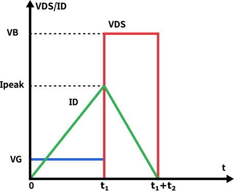
The circuit starts working,InAt time 0, giveDevice under testDUTAdd a certain pulse with a pulse width oft1, Make the device conductive,The circuit is conducting simultaneously,At this time, the power supply voltageVDD charges the load inductor L, and its current change rate is:

InAt time t1, the current on inductor L reaches its maximum value Ipeak, and the stored energy also reaches its maximum:

It can be seen that inductive energy storage is closely related to the following three factors: inductance value LLL、 Power supply voltage VDDV_ {DD}VDD , and pulse width t1t_1t1.
When the pulse lasts until At time t1t_1t1, the gate voltage suddenly drops to 0, and both the DUT (device under test) and the switching transistor turn off simultaneously. At this point, the spin electrons in the inductor that were originally in a steady state enter a non steady state due to current interruption,Spin magnetic moment changes.
Due to the coil structure of inductors, the electron orbital magnetic moment suddenly disappears at the moment of current interruption, resulting in a sudden change in spin magnetic moment and the release of magnetic field. This change triggers the magnetoresistance effect, causing electrons to start moving in reverse in an attempt to quickly return to a new steady state.
At this point, the inductor begins to discharge in reverse, exhibiting its energy storage effect.MOSFET is equivalent to a large resistor at this stage, and the speed at which the inductor releases energy is very fast, resulting in drastic changes in current.
In order to release the energy stored in the inductor, the inductor will generate an induced voltage VBV_BVB, This voltage may be higher than the rated avalanche breakdown voltage (BVDSBV) of MOSFET_ {DS}BVDS )Usually 1.3 times its size. This is because the device absorbs energy and generates heat during EAS (Single Pulse Avalanche Energy) testing, resulting in an increase in junction temperature, and the avalanche breakdown voltage has a positive temperature coefficient.
Ultimately, this higher induced voltage may trigger The body diode of MOSFET undergoes avalanche breakdown to release energy from the inductor.
We can obtain:

ifMOSFET can withstand the avalanche energy without damage. After a certain period of time, all the energy in the inductor will be released, and the current in the circuit will also drop to zero. At this point, by integrating the voltage and current of the MOSFET, the value obtained is the EAS energy that the MOSFET is subjected to, which is exactly equal to the energy stored in the inductor.
Next, let's take a look at another type of testing circuitB:

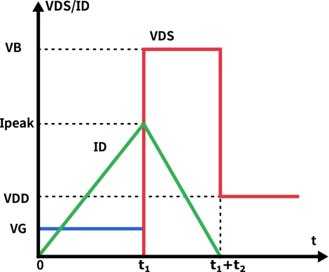
In this type of testing circuitAt this point, the inductance voltage is no longer simplyMOSFET induces voltage VB, but VB-VDD, didt, and current drop time t2 all need to change. The EAS calculation formula is:

From the measurement results, it can be seen that the circuitThe EAS measurement value of B is higher than the energy storage value of the inductor itself, because the measurement model incorporates the energy contribution of the power supply voltage VDD into the calculation system.
In terms of circuit topology and computational logic, circuitsAlthough the architecture design of A is relatively complex, it is simpler in EAS calculation - its energy model only needs to consider the energy stored in inductors; Although circuit B has a simpler topology, it is actually more cumbersome in the EAS calculation process: on the one hand, it requires real-time monitoring of the VB voltage signal, and the actual waveform of this voltage shows a non ideal fluctuation state, which differs from the smooth curve in the theoretical schematic diagram; On the other hand, since VDD is always connected to the energy release circuit, when the device fails due to a short circuit, the circuit current will sharply rise to the dangerous threshold. Therefore, overcurrent protection devices must be configured to avoid the risk of power short circuit.
From the above analysis, it can be concluded that the size of inductive energy storage is influenced by the amount of inductanceL、 The three parameters of power supply voltage VDD and pulse width t1 have an impact. In engineering practice, if it is necessary to increase energy storage, a fixed VDD and L method is usually used to achieve energy increase by extending the pulse width (as increasing inductance involves complex processes such as core selection and winding design), until the energy value at which the device just maintains normal working state is EAS.
Targeting different devicesEAS horizontal comparison requires the establishment of a unified measurement benchmark (usually based on inductance L as the unified standard). This is because the energy release rate (i.e. current drop rate di/dt) will change with the change of inductance: the larger the inductance, the smaller the peak avalanche current and di/dt, the longer the energy release period, the longer the device's heat dissipation time, and thus the larger the EAS measurement value. If there is a lack of unified inductance standards, it will result in differences in the energy release dynamics of different devices, affecting the comparability of test data.
4Reason for failure
InIn EAS testing, the core mechanism of MOS device failure is thermal breakdown failure (i.e. junction temperature reaching the intrinsic temperature threshold). From the perspective of failure causes, the primary factor may be the insufficient heat dissipation performance of the packaging structure; After excluding packaging failure factors, the failure mechanism can focus on the device body and can be physically divided into two categories: current wire breakdown failure and failure caused by parasitic bipolar junction transistor (BJT) conduction.
① Mechanism of current wire breakdown failure
Under normal operating conditionsDuring the EAS process, due to the thermal effect of avalanche current and the positive temperature coefficient characteristics of breakdown voltage (BV), avalanche current will dynamically transfer between different transistor units, eventually reaching a critical value in a local area. When the dynamic transfer mechanism of the current wire fails, local thermal breakdown will occur. If there are structural defects in the device (such as abnormal unit structure, low breakdown voltage in the terminal area, etc.), it will lead to abnormal concentration of avalanche current at the defect site, thereby causing the EAS test value to be lower than the normal level.
The core of this failure mode lies in the control of current uniformity. All transistors can essentially be regarded as variable resistance elements, and current tends to flow towards paths with lower resistance. Therefore, it is necessary to optimize the withstand voltage characteristics of the avalanche current path, which involves regulating the electric field distribution under avalanche conditions. When the avalanche current density reaches a high level, the migration concentration of charge carriers can be comparable to the substrate doping concentration, thereby changing the effective doping concentration of the substrate and ultimately affecting the distribution of electric field and current density in the depletion region.
② Mechanism of parasitic BJT conduction failure
The physical structure of MOSFET naturally includes a parasitic NPN bipolar transistor consisting of an N source region, a P-base body region, and an N-drift region (corresponding to the emitter, base, and collector of the BJT, respectively). Although the parasitic effect of BJTs can be suppressed by short circuiting the P-base region with the source through ohmic contact, it cannot be completely eliminated due to the limitations of the process structure.
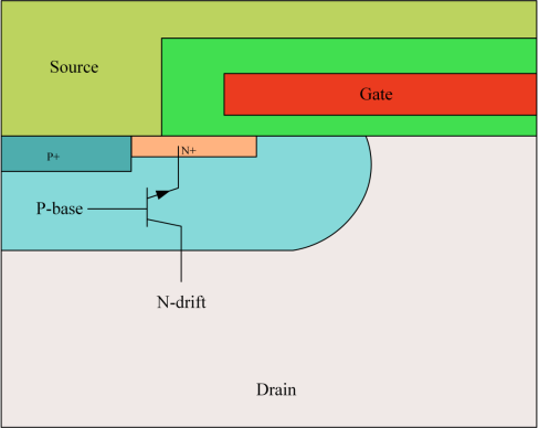
In the avalanche breakdown state, the reverse saturation current is amplified by the avalanche effectM times, electrons flow to the drain and holes flow to the source,As shown in the figure:
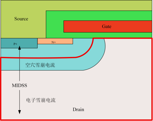
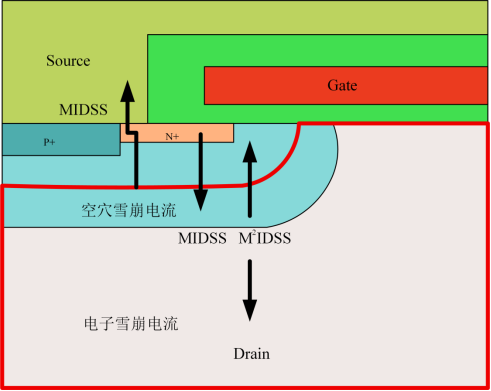
In There are two path options for hole transport below the N source region: one is to exit from the source through the P-base region, and the other is to exit from the source through the N region. The specific flow of holes is determined by the resistance values of two paths - when the hole potential is lower than the forward conduction threshold voltage (i.e.<0.7V) of the PN junction formed by the P-base region and N region, all holes will flow out of the source along the P-base region, and the parasitic BJT is in a cut-off state. The device breakdown voltage is maintained at the base collector breakdown voltage BVCBO when the emitter is open circuited; When the hole potential is sufficient to make the PN junction conduct forward (i.e.>0.7V), electrons in the N region will be injected into the P-base region, and this current will be amplified M times by the avalanche effect, triggering parasitic BJT conduction. At this point, the breakdown voltage of the device transitions to the emitter collector breakdown voltage BVCEO when the base is open circuited. Due to the current entering the positive feedback amplification state, the device will quickly experience thermal failure.
So, in order to suppress parasitismThe key to increasing EAS by turning on BJT is to reduce the resistance value on the path from avalanche current (hole current) to the contact hole. Here are some examples:
a.reduceN area;
b.increaseP-base doping concentration, injecting heavily doped P regions;
c.optimizeContact resistance between P-base and metal
5Conclusion
In practical applications,EAS mainly describes the energy of a single avalanche.
However, there is another parameter in the device manual EAR, The energy limit for repeated avalanche breakdown is usually much lower than EAS, and its impact on chip performance is relatively small.
Therefore, in the design, efforts should be made to avoid large amounts of energy as much as possibleThe occurrence of EAS is to protect the long-term reliability of the device.
EAS, as a key indicator for evaluating the avalanche energy tolerance of MOSFET devices, not only provides a quantitative reference for device performance for designers, but also helps to avoid potential overvoltage damage in practical applications.
Taiyi Semiconductor Co., Ltd. focuses on markets such as consumer electronics, new energy, and intelligent manufacturing, providing customers with high-quality and highly reliable power semiconductor products.
The product categories include power management analog integrated circuit chips, power discrete devices, andSiC and other new material devices provide customers with complete power solutions.
 CN
CN EN
EN